Microscope technology: an exceptional instrument arriving soon at Grenoble INP - UGA
Research, Innovation
On December 9, 2022

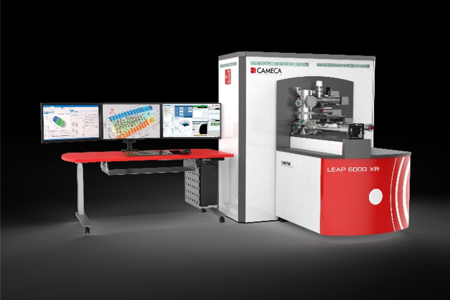
As part of the 2021-2027 CPER*, Grenoble INP - UGA is leading a project to acquire some exceptional equipment: a tomographic atom probe. This recent model will be the first new-generation instrument in France and the second in Europe, and features new functionalities. It will be installed in the SIMAP laboratory and managed by the CMTC**.
The concept of the atom probe was born in the 1990s, with particular contributions from the Rouen Groupe de Physique des Matériaux (GPM), which developed one of the first models. Nowadays, there are four in France, in laboratories in Rouen and Marseille, as well as at the CEA Grenoble and Saclay, some of which are from a fairly old generation. The Grenoble project, which combines Grenoble INP - UGA, the CEA and other laboratories in the Auvergne-Rhône-Alpes region, plans to acquire two pieces of equipment: a latest-model atom probe featuring new functionalities, and a focused ion beam (FIB) instrument, which is able to analyse samples using a tiny tip with the radius of curvature measuring a few tenths of a nanometre.
Atom probe tomography is a 3D, high-definition analysis technique, which makes it possible to observe the spatial distribution of atoms in a given material. It works by evaporating atoms, in the form of ions, at the surface of a sample using an intense electrical field. “In a way, the sample is used like a lightning rod that attracts lightning,” explains Alexis Deschamps, researcher at SIMAP*** and professor at Grenoble INP – Phelma, UGA. “Placed in a vacuum at a temperature near absolute zero, the sample is subjected to an electrical field that is intensified at the tip, and tears away the atoms one by one.”
As the electrical field is applied in the form of very short pulses, the sample is evaporated atom by atom, atomic layer by atomic layer. The ionized (and therefore charged) atoms are accelerated in the ambient electrical field and collected by a 2D detector. The chemical nature of each atom is determined according to the time of flight for the ions to reach the detector. Furthermore, each atom’s original position in the sample is determined according to where the ion arrives on the detector using inverse projection. “We therefore obtain a map of atom distribution in the sample with 3D atomic resolution. The machine is able to reconstruct 10 to 100 million atoms in a few hours.”
The newest version of the instrument combines the pulses of a femtosecond laser in UV with electrical pulses. This makes it possible to analyse almost all materials, from metal alloys to nonconductors: rocks, ceramics, semiconductors, nitrides, oxides, and even liquid electrolytes from batteries solidified by the cold. The laser’s wavelength, which is smaller compared to previous generations, limits the tip from warming up and therefore reduces atom movement before they evaporate, improving the instrument’s resolution. The combination of electrical and laser pulses is unique in France, and allows for more efficient ionization in materials that are known to be difficult to measure.
The project partners already have ambitions for use in the fields of metallurgy, microelectronics, nanoscience and geology. “One possible use is for recycling materials. When we recycle, we mix materials and we find ourselves with undesirable chemical species that get lodged in crystalline defects,” explains Alexis Deschamps. “The atom probe may help us understand how potentially damaging these defects can be. Another example is in geology, where the technique is used to carry out isotopic analysis, for dating for example, or to study deformations, blends and eventually, the rock’s history.”
To be analysable, the samples must be prepared in the form of nanometric tips using a specific FIB workstation, which is being acquired as part of the same contract. The two pieces of equipment, representing a total investment of €4.2 million, will be hosted at SIMAP, managed by CMTC from May 2023, and accessible for the establishment’s industrial and academic partners, as well as the research community in the Auvergne-Rhone-Alpes region more broadly.
Atom probe tomography is a 3D, high-definition analysis technique, which makes it possible to observe the spatial distribution of atoms in a given material. It works by evaporating atoms, in the form of ions, at the surface of a sample using an intense electrical field. “In a way, the sample is used like a lightning rod that attracts lightning,” explains Alexis Deschamps, researcher at SIMAP*** and professor at Grenoble INP – Phelma, UGA. “Placed in a vacuum at a temperature near absolute zero, the sample is subjected to an electrical field that is intensified at the tip, and tears away the atoms one by one.”
As the electrical field is applied in the form of very short pulses, the sample is evaporated atom by atom, atomic layer by atomic layer. The ionized (and therefore charged) atoms are accelerated in the ambient electrical field and collected by a 2D detector. The chemical nature of each atom is determined according to the time of flight for the ions to reach the detector. Furthermore, each atom’s original position in the sample is determined according to where the ion arrives on the detector using inverse projection. “We therefore obtain a map of atom distribution in the sample with 3D atomic resolution. The machine is able to reconstruct 10 to 100 million atoms in a few hours.”
The newest version of the instrument combines the pulses of a femtosecond laser in UV with electrical pulses. This makes it possible to analyse almost all materials, from metal alloys to nonconductors: rocks, ceramics, semiconductors, nitrides, oxides, and even liquid electrolytes from batteries solidified by the cold. The laser’s wavelength, which is smaller compared to previous generations, limits the tip from warming up and therefore reduces atom movement before they evaporate, improving the instrument’s resolution. The combination of electrical and laser pulses is unique in France, and allows for more efficient ionization in materials that are known to be difficult to measure.
Applications in all fields
3D reconstruction of a sample can be useful to create architectural materials on a nanometric scale responding to specific properties (mechanic, electric, etc.) according to the target application. It can also be used to see how a material evolves during manufacturing and use, in order to understand its durability.The project partners already have ambitions for use in the fields of metallurgy, microelectronics, nanoscience and geology. “One possible use is for recycling materials. When we recycle, we mix materials and we find ourselves with undesirable chemical species that get lodged in crystalline defects,” explains Alexis Deschamps. “The atom probe may help us understand how potentially damaging these defects can be. Another example is in geology, where the technique is used to carry out isotopic analysis, for dating for example, or to study deformations, blends and eventually, the rock’s history.”
To be analysable, the samples must be prepared in the form of nanometric tips using a specific FIB workstation, which is being acquired as part of the same contract. The two pieces of equipment, representing a total investment of €4.2 million, will be hosted at SIMAP, managed by CMTC from May 2023, and accessible for the establishment’s industrial and academic partners, as well as the research community in the Auvergne-Rhone-Alpes region more broadly.
* Government-region planning contracts (CPER) represent a development tool between the national government and the regions, by implementing structural projects. CPERs aim to strengthen development policy in support of equality between the territories.
**Consortium des Moyens Technologiques Communs (technology platform for characterising materials)
***CNRS, Grenoble INP – UGA, UGA
**Consortium des Moyens Technologiques Communs (technology platform for characterising materials)
***CNRS, Grenoble INP – UGA, UGA
Published on December 13, 2022
Updated on December 13, 2022
Updated on December 13, 2022

